The scanning electron microscope allows one to obtain nice images, or to draw nanostructures. The beam can also be used for physical measurements: for instance, the measure of the e-beam induced current (EBIC) is a convenient way of analyzing carrier diffusion properties in semiconductors. In collaboration with CRN2 at Sherbrooke University (Quebec), we have performed a series of high spatial resolution EBIC measurements on silicon nanowires.
Let us consider a silicon nanowire topped by its catalyst. In the microscope chamber, it is contacted by microelectrodes (“micromanipulators”), one (being deposited on) in contact with the gold catalyst and the other on the cleaved facet of the silicon substrate (Figure). Let us then sweep the electron beam along the nanowire length as if we wished to make a scanning electron image. During the sweeping, electron-hole pairs are created within the nanowire by the electron beam. In regions where there is (an electric field) a potential gradient (
e.g. p-n or Schottky junctions), carriers of opposite charges spontaneously separate and flow in opposite directions.
That occurs, for instance, in the depletion region at the interface between the silicon nanowire and its gold catalyst. With the two electrodes and an ammeter, the induced current that is locally created in the depletion region and its surroundings can be measured (Figure). This gives us the width of this zone: W=150 nm. One can also deduce the diffusion length of the carriers along the wire axis, L=200 nm, which is a difficult quantity to access by other techniques.
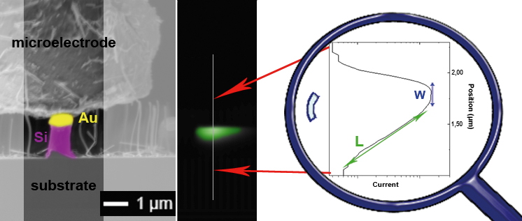
Left: SEM image of the nanowire and its contacts.
Center: corresponding EBIC image.
Right: EBIC current profile along the central axis of the nanowire.