The question of the integration of a truly monolithic group IV (GF) laser source on silicon has long been considered as a major hindrance for the development of silicon photonics. While it was repeatedly the object in the past decades of premature announcements, recent results definitely made the raise of a group four laser a reality. Our group, in close collaboration with the CEA-LETI institute, is fully involved in the research on GF sources, and is now among the three main gamers in the field. For the period 2015-2019, our investigations cover two axes, and start from the understanding of the physics at stake in the materials to the realization of GF lasers.
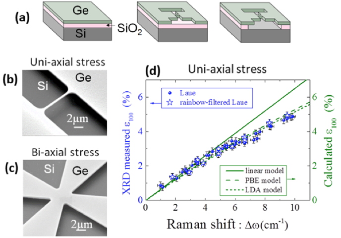
Figure 1: (a) device fabrication steps, (b), (c) microbridges and microcrosses for uniaxial and biaxial strain induction and (d) experimental (blue dots) and theoretical (green lines) strain-Raman shift relation for <100> uniaxial strain
[1, 2].
 On the road to the Ge laser
The peculiar structure of Ge, with a modest indirect to direct band gap energetic offset, makes this semiconductor particularly appealing for light emission purposes on Si, as Ge is routinely integrated in CMOS processes. Indeed, tensile strain along the <100> direction or along the (100) plane reduces the band gap offset and even makes Ge transiting from an indirect to a direct band gap configuration (predicted at around 5.5% for uniaxial <100> load and 2% for (100) biaxial load). This guided our first efforts towards a customized platform developed at CEA-LETI, the optical Germanium On Insulator (GOI), made of a micronic Ge layer in a slight residual tensile strain state and transferred onto a thick (1 µm) buried oxide. We applied the strategy of strain redistribution and induction into micrometric constrictions. The accumulated residual strain contained in adjacent «arm strain reservoirs » is released during the arm under-etching, and further transferred and enhanced in the central area, Figure 1a. Applying this approach to uniaxial and biaxial geometries (see in Figure 1b and c), led to massive tensile straining of Ge. Our group obtained the highest uniaxial and biaxial strains reported to date at room temperature with
ε(<100>)=4.8% and
ε((100))=2%. Very significant volumes of Ge, over sections capable of sustaining optical modes, are strained at unprecedented levels. This motivated a set of materials studies on our side to evaluate the potential of strained Ge as a gain material. In that respect, a combined micro Raman-X ray micro diffraction study conducted on highly strained Ge bridges showed significant deviations at high strain of the actual vs predicted Raman shift, thereby setting a new standard for this law (Figure 1d). In the same spirit, we tackled the question of the deformation potentials in highly strained Ge
via micro-electroabsorption measurements (Figure 2a). This was done at the waveguide level and allowed us to reevaluate these constants, together with an estimate in the change of the oscillator strength of vertical transitions with the light and heavy hole bands (LH, HH), giving very valuable information for designing Ge lasers (see in Figure 2b to d). Our group developed an in depth expertise in the design and microfabrication of Ge microresonators on the Plateforme Technologique Amont (PTA), at the frontier between optics and MEMs technology, but also enriched it's know how on the spectroscopic side with the development of new spectroscopic and original characterization benches running in the 2-5 µm range.
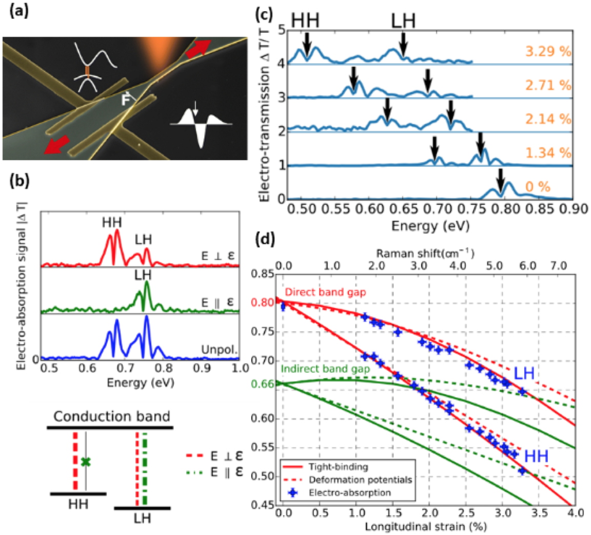
Figure 2: (a) Schematics of a probed, strained, microbridge in our differential spectroscopy set up, (b) evidence of the different polarization sensitive transitions between conduction band and LH, HH band edges (c) electrotransmission spectra of microbridges at different strain levels (d) strain dependance of the HH-LH band gap splitting compared with predictions from the « deformation potential » and tight binding models
[3].
GeSn lasers
The recent development of new strategies of crystal growth led to the synthesis of out of equilibrium, Sn rich, Ge
(1-x)Sn
x alloys, which, contrary to Ge, were predicted a long time ago to be "as grown" direct band gap materials for reasonably low tin contents (between 6 and 12%, depending on the residual strain state). This remarkable and unique feature for a GF alloy made very opportune launching research activities on GeSn lasers in collaboration with the LETI institute. Very rapidly, our partner grew thick GeSn epilayers on Ge buffers on whole 8 inches wafers, at the state of the art,
i.e. with a high crystalline quality and a high tin content. In an attempt to reach laser oscillation, our group fabricated the first "primitive" microdisk resonators, made of an optically active, disk shaped GeSn layer lying on a smaller diameter Ge pedestal (see in Figure 3a). We demonstrated laser operation under pulsed excitation in homogeneous layers of 13 and 16% Sn content, but also in step concentration graded layers reaching top concentrations of 13 and 16% (Figure 3b), with the emission wavelength spanning the 2.6 to 3.1µm range (Figure 3c). Thresholds were found to be high (of the order of 400 kW/cm
-2 at 25K for the 16 % layer) and the limit operation temperature at 180K, both competing very well at that time with the device performances of the Julich leading group. A great improvement in the laser performances is obtained by confining the carriers in a well inserted within a GeSn heterostructure made of different tin content layers, but also by adding ternary SiGeSn alloys barriers (see in Figure 3d). When processed under our model microdisk resonator, this results in an increased limit operation temperature (230K) and decreased thresholds (130 kW/cm
-2 at 15K) of the 16 % active layer, constituting a new performance breakthrough (see in Figure 3e).
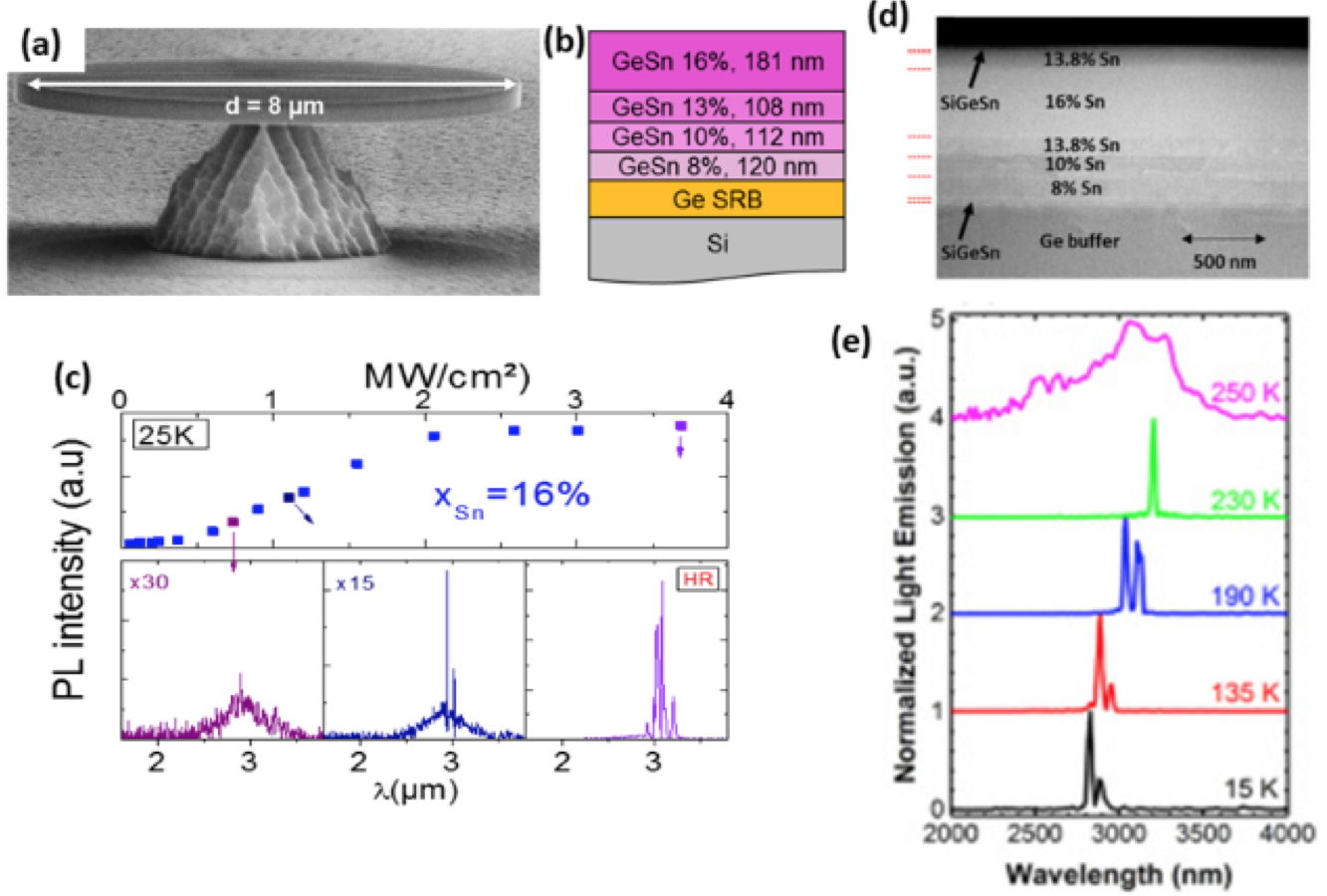
Figure 3: (a) typical GeSn microdisk resonator on a Ge pedestal, (b) step concentration graded GeSn stack and (c) lasing spectra and associated Lin-Lout curve at 25K for the 16% sample, (d) cross section of a GeSn heterostructure with the 16% Sn active layer and (e) laser effect evidenced at 230K
[4, 5].
Laser operation is also clearly demonstrated in other classes of resonators, such as photonic crystals made of an array of holes in a free standing GeSn membrane (see in Figure 4a and b). Enhanced light-matter interaction is triggered at band edge points of the photonic band diagram and gives rise to laser action (see in Figure 4c and d). This unambiguously shows the robustness of the laser effect in our layers and testifies to the clear and significant gain in this material.
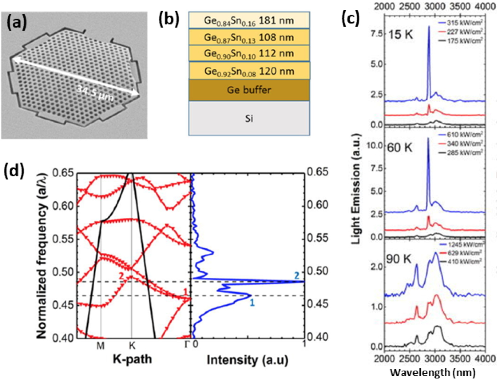
Figure 4: (a) top view of a GeSn photonic crystal membrane on Si, (b) step graded GeSn stack, (c) PL spectra at different temperatures and powers and (d) correlation lasing line-photonic band edge
[6].
References
[1] Gassenq A, Guilloy K, Pauc N, Hartmann JM, Osvaldo Dias G, Rouchon D, Tardif S, Escalante J, Duchemin I, Niquet YM, Chelnokov A, Reboud and Calvo V Study of the light emission in Ge layers and strained membranes on Si substrates.
Thin Solid Films, 2016,
613(2016): 64-67
[2] Gassenq A, Tardif S, Guilloy K, Dias GO, Pauc N, Duchemin I, Rouchon D, Hartmann JM, Widiez J, Escalante J, Niquet YM, Geiger R, Zabel T, Sigg H, Faist J, Chelnokov A, Rieutord F, Reboud V and Calvo V Accurate strain measurements in highly strained Ge microbridges.
Applied Physics Letters, 2016,
108: 241902
[3]
[4] Reboud V, Gassenq A, Pauc N, Aubin J, Milord L, Thai Q, Bertrand M. Guilloy K, Rouchon D, Rothman J. Zabel T, Armand Pilon F. Sigg H, Chelnokov A, Hartmann J and Calvo V
Optically pumped GeSn micro-disks with 16% Sn lasing at 3.1 µm up to 180 K.
Applied Physics Letters, 2017,
111: 092101
[5]
Thai QM, Pauc N, Aubin J, Bertrand M, Chrétien J, Delaye V, Chelnokov A, Hartmann JM, Reboud V and Calvo V
GeSn heterostructure micro-disk laser operating at 230 K.
Optics Express, 2018,
26(25): 32500-32508
[6] Thai Q, Pauc N, Aubin J, Bertrand M, Chrétien J, Chelnokov A, Hartmann J, Reboud V and Calvo V
2D hexagonal photonic crystal GeSn laser with 16% Sn content.
Applied Physics Letters, 2018,
113(5): 051104