.
| | The SiNaPS team investigates the new physical phenomena appearing when silicon and group IV based semiconductors are down-sized to the nanometer scale. Our effort is tightly focused on two fields: the physics of silicon and germanium based nanostructures (i.e. nanowires, quantum boxes and nanostructured Si or Ge based alloys) and the optics of wavelength-scale optical microstructures like photonic crystals and microcavities. The team activities include material growth, clean room nanofabrication and optical characterization. The team has also a long tradition of trying to push its commitment up to proof of concept or demonstrators level when the scientific maturity of a topics allows for in order to to unveil future potential applications. His research as so far lead to times to the launch of starut-ups based on its scientific background and achievements
|
|
 Main achievements and current research axes
 Among the main achievements are, in the field of group IV nanostructures, the growth of sub-5 nm diameter crystalline Si and Ge nanowires, the growth of nanostructured (branched) silicon nanowires, the nanofabrication of porous alumina templates, the growth of nanostructured GeMn alloys containing a high T
c (>400 K) ferromagnetic phase.
At the frontier of electronics and optics, we studied the mechanisms of carrier recombination and light emission in silicon-on-insulator (SOI) thin films where we demonstrated the Fermi-Dirac condensation of excitons into a metallic liquid.
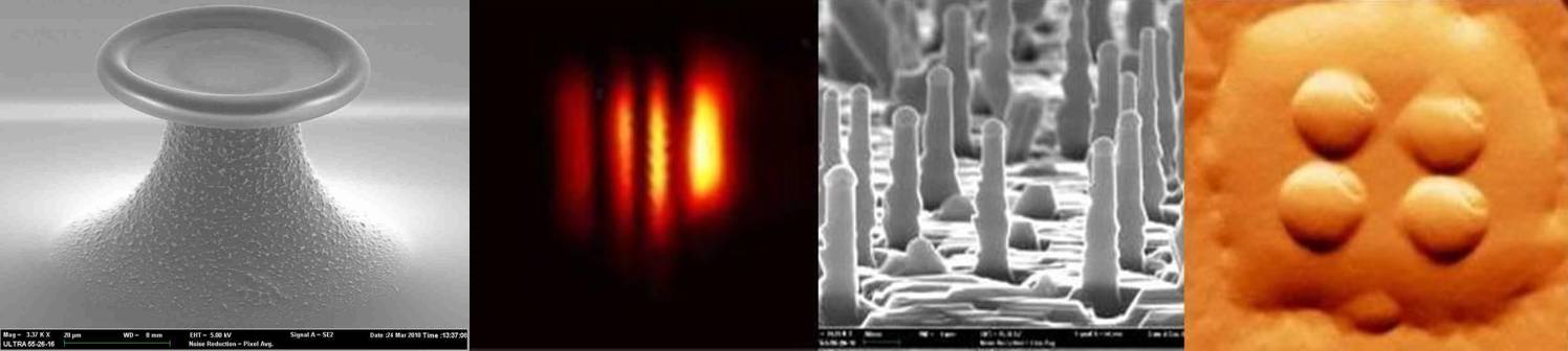
In the field of photonic crystals and microcavities, we first evidenced the potential of SOI based structures to control the radiation diagram of photons. We then demonstrated strong (2 orders of magnitude) light extraction enhancement by low group velocity SOI photonic crystals. Finally, we applied our effort to the quest for ultra-strong light confinement in high Q nanobeam cavities (Q > 60.000 for V = 0.6(l/n)
3 achieved).
We then focused towards on-chip optical tweezing where we achieved trapping and on-chip light manipulation of sub-wavelength sized nanocolloids en lightning enhanced optical forces. We moved the cursor one step further by investigating the possible “manipulation” of living cells or bio-material by interaction with on-chip optical nanotweezers. A first milestone was to achieve the optical non-destructive trapping of living material: bacteria. And a second was to evidence the possibility of bacteria identification though their near-field interaction with the photonic crystal nanobeam cavity.
In the field of silicon-compatible lasers, the breakthrough has been the demonstration of laser emission from Ge and GeSn alloys. A first goal was to evidence the presence of gain at the direct band gap of strained and highly doped Ge thin films and/or GeSn alloys. The next one was to combine this material with optical resonant cavities in order to reach the stimulated emission regime. Our work lead to the demonstration of room temperature laser emission.
Finally, the team made also strong contributions to the field of energy storage and thermal transport at the nanoscale through intensive collaborations with two neighbouring teams. Among them are nanowires and quantum dots for energy production in PEMFC, for energy harvesting with thermoelectric devices and for energy storage in super-capacitors.
 Research tools
 To reach its goals, SiNaPS is committed to the epitaxial growth by MBE and by CVD of the following materials: Si, Ge, SiGe, GeSn, GeMn. The team is highly involved as well in the development of nanofabrication process of SOI, GeOI photonic bandgap devices on the Upstream Nanofabrication Facility (PTA). The third pillar of SiNaPS activity consist of the spectroscopy of those nanostructures where the lab has developed an extensive background and many original tools such as: spatially-resolved spectroscopy, photocurrent measurements at micron scale, wave-guided spectroscopy, evanescent coupling spectroscopy, near-field optical spectroscopy and and a low temperature STM (with in-situ growth capabilities).