Nowadays, silicon is seen as a material of choice for developing quantum technologies on the basis of advanced manufacturing processes developed over the last decades for electronic as well as for photonic integrated circuits. While the development of quantum processors based on spin qubits in Si is under way at several institutes including CEA Grenoble, Si quantum photonic chips are attractive for quantum simulations and –in a long-term perspective– for the development of large-scale quantum networks. The processing of quantum states of light with a high fidelity, as well as the high efficiency detection of single photons using integrated superconducting nanowire detectors have been demonstrated on Si photonic chips. By contrast, the generation of quantum states of light on demand has remained elusive. For this reason, either non-deterministic sources of quantum light (based on four wave mixing in Si) or the combination of GaAs based single-photon sources and Si photonic chips have been used until now, with strong penalties in terms of scalability and/or functionality.
The recent demonstration of a single-photon source embedded in silicon by the ANR OCTOPUS consortium (L2C Montpellier, LM2NP Marseille and our laboratory) and coworkers (U. Leipzig, U. Oslo, IRIG/MEM) might change this situation radically. The authors have studied punctual defects, formed inside a commercial silicon-on-oxide wafer through implantation of dilute carbon atoms and thermal annealing. Although known since the 1970’s as the “G-centers” of silicon, such defects are studied here for the first time at the single defect level. Isolated G-centers behave as bright artificial atoms, which are able to emit photons one by one at a telecom-compatible wavelength (~1.28 µm) and with a high quantum efficiency. Further studies focus on the integration of isolated G centers within SOI microcavities and on the exploration of their spin properties, so as to develop two key devices for photonic quantum engineering: single-mode single-photon sources and spin-photon interfaces integrated within SOI photonic chips. Let us finally note that the theoretical study of the “G-center” at
MEM is a long and ongoing research, which started with the BOLID ANR project (2010-2013) originally devoted to solar grade silicon.
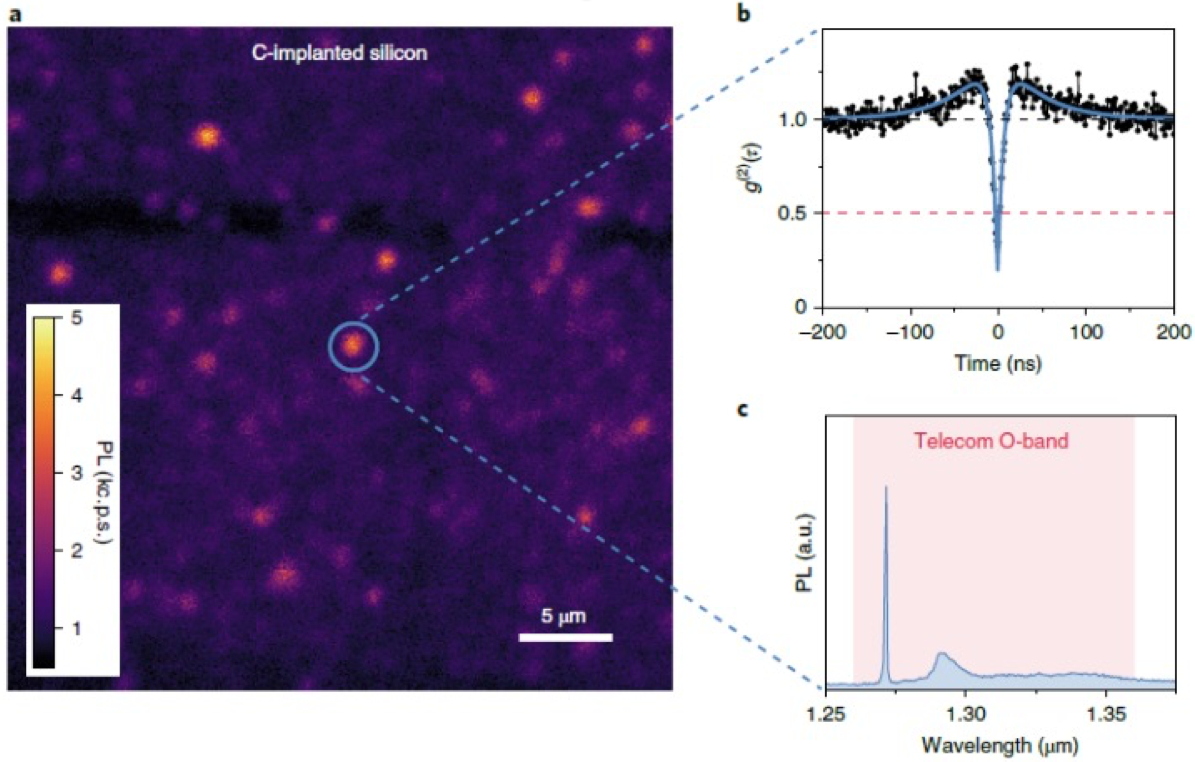
Legend: (a) Fluorescence map of a thin layer of silicon on SiO
2, containing a dilute ensemble of G-centers. (b) A clear antibunching behavior, observed on photon correlation histograms, confirms that each emission spot corresponds to a single emitter and demonstrates the ability of isolated G-centers to emit photons one-by-one. (c) Emission spectrum of a single G-center showing a main line in the telecom O-band.