The development of semiconductor nanowires has inspired new devices where the low dimensionality and the large surface-to-volume ratio play a key role in the overall performance. In the domain of optoelectronics, nanowire geometries are particularly interesting for flexible electronics, or for the implementation of on-chip optical interconnects. The capabilities of nanowires as photodetectors are being investigated for different material systems. Nanowires present a large dielectric mismatch with their surroundings, and their diameter is generally smaller than the detected wavelength. These interesting features allow the engineering of the refractive index or the electrical cross section (i.e. the capacitance), while maintaining the absorption characteristics of the bulk. Photocurrent in nanowires can be activated via either (i) generation of electron-hole pairs by absorption of photons with energy larger than the semiconductor band gap (interband transitions), or (ii) electron transitions between quantum-confined energy levels in the conduction band of heterostructures (intersubband transitions), by photons whose energy is resonant with the electronic transition, which is in term determined by the geometrical dimensions of the heterostructure. The GaN/AlN material system is well adapted for both processes. The direct band gap of GaN is particularly adapted for visible-blind interband photodetection in the ultraviolet spectral range, and intersubband transitions in GaN/AlN heterostructures can be tuned to cover the 1.55 µm near-infrared telecommunication wavelength. Besides, compared to other materials, GaN presents the advantage of being physically and chemically robust, which enables operation in extreme environments.
At NPSC, in collaboration with CNRS-Institute Néel, we are able to fabricate photodetectors consisting of a single GaN nanowire containing GaN/AlN heterostructures. These nanowires can be isolated and contacted on a silicon nitride membrane, which allows the observation of the device by transmission electron microscopy. We have engineered the heterostructure dimensions and the doping profile in these nanowires to enhance its interband photoresponse at low bias. This has led to the successful demonstration of visible-blind UV-B photodetectors operating at < 1 V bias with a responsivity enhancement of two orders of magnitude in comparison with previous literature. Furthermore, with our GaN/AlN heterostructure design adapted for intersubband absorption, we have demonstrated the first intersubband photodetector in a nanowire, which operates in the 1.55 µm telecommunication band.
PHELIQS was in charge of the nanowire design, growth and optical/electrical characterization. This work benefited from access to the Nanocharacterization platform (PFNC) at CEA Minatec. Membrane production and nanowire contacting were carried out at the Nanofab cleanroom of Institut Néel. The work on UV photodetection was performed in collaboration with Justus Liebig Universität Giessen in Germany.
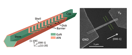
Figure. Schematic description of a GaN/AlN nanowire photodetector, together with a scanning electron microscopy (SEM) image of one of the devices. In the SEM image, parallel green lines mark the presence of the GaN/AlN heterostructure.