Nanowire conductivity increases drastically under ultraviolet excitation (wavelengths shorter than 360 nm) polarized along the nanowire main axis. In contrast, no response is measured under visible (blue, green or red) excitation. This blindness in the visible spectrum is a particularity of nitride semiconductor based photodetectors. When the GaN is grown as a thin film, the contrast between the ultraviolet and the visible absorptions is around 1,000. Now with GaN nanowires, this contrast reaches 1,000,000, due to their exceptional crystalline quality. Another advantage of the nanowire photodetectors is their response time in the millisecond range, while a photocurrent can persist during minutes or even hours in the case of thin films.
We now will study heterostructured nanowires in order to increase the photoconduction gain. Once the single nanowire response has been optimized, we will fabricate organized matrices of nanowires, the ultimate goal being the fabrication of high resolution imaging devices that mimic the human retina.
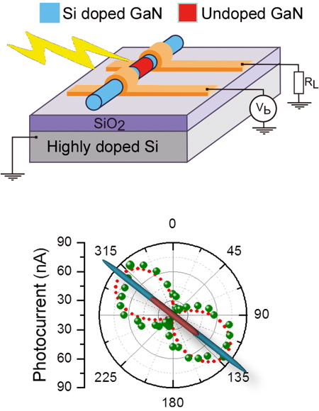
Photocurrent measurement principle and intensity variation as a function of the angle between the nanowire axis and the linear polarization of the incident light. The figure of 8 is characteristic of the light coupling with the nanowire. In the background: micrograph of MBE-grown GaN nanowires.