Light sources fully integrated into microelectronics technology are the missing stones of silicon photonics. Silicon, as well as germanium, are not well suited for light emission in their natural form, due to the indirect nature of their bandgap. In the case of Ge, this limitation can potentially be lifted through the application of tensile strain: theoretical studies predict a direct bandgap for Ge, for a tensile strain of the order of some per cents. Germanium being widely used in microelectronics, the demonstration of a Ge source on a Si chip would be a major step forward for silicon photonics.
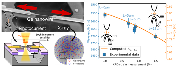
We have shown that it is possible to strain a germanium nanowire in a mastered way by applying mechanically a tensile uniaxial stress. X-ray Laue microdiffraction experiments, which have been performed on the BM32 beamline at ESRF, have been used to measure the strain inside the nanowire, reaching up to 1.5 % along its axis. Photocurrent spectroscopy experiments reveal a strong decrease of the energy separation between the direct and indirect bandgaps of Ge, in accordance with theoretical predictions.
We currently develop Ge membranes experiencing even stronger tensile strains, ranging between 2% and 5%, starting from "Germanium on Insulator" (GeOI) wafers from CEA/Léti. For these target values of the strain, the Ge membrane should display a direct band gap, enabling optical gain upon optical or electrical excitation, and ultimately the demonstration of strained Ge lasers on a Si chip.
Work performed within the “Projets Phares DSM-DRT” “Photonics” and "Operando".
Ge nanowire (diameter: 250nm, length: 10 µm) in the straining micromembrane device.
µPhotocurrent and µXray diffraction experiments.
Evolution of electronic states with tensile strain.