The development of semiconductor nanostructures has been achieved through a good control of their fabrication, for instance by Molecular Beam Epitaxy (MBE). For a long time, this technique has been limited to the growth of planar structures such as quantum wells, inducing a spatial confinement of charge carriers in the perpendicular direction. New challenges, such as the realization of single-photon emitters for quantum communications, require a stronger confinement in two or three directions, obtained by making nanowires and quantum dots.
The growth of nanowires is usually seeded by a liquid droplet of a few nanometers, which determines the diameter of the nanowire. During the growth, quantum dots can be inserted by changing abruptly the composition of the molecular beam. This “Vapor-Liquid-Solid” mechanism combines a vapor phase in the beam, a liquid phase in the droplet, and a solid phase in the nanowire. At the seed-nanowire interface, the growth was supposed to take place through the nucleation of a one-monolayer step and its propagation along this interface. For years, this was a mere assumption. The Nanomax setup operated in Palaiseau and first applied to GaAs nanowires by our colleagues from the Centre for Nanoscience and Nanotechnology now allows to observe this process in-situ in a modified electron microscope.
In our group, we are interested in II-VI semiconductors combining a metal such as Zn or Cd (column II of the Mendeleev table) and a chalcogen such as Se or Te (column VI). These materials are particularly interesting as active optical elements, for light emission or photovoltaics. II-VI nanowires can be grown with a gold seed which is solid and crystalline instead of liquid: this is the “Vapor-Solid-Solid” growth, which is expected to provide sharper interfaces when inserting a quantum dot. Observing the growth of ZnTe nanowires at Nanomax revealed two original aspects: the role of the lattice mismatch at the nanowire-seed interface, and a self-regulation of the step dynamics.
Gold and ZnTe crystals feature the same Bravais lattice, but the ZnTe unit cell is 3/2 larger than that of gold. When the gold monolayer located at the interface is progressively replaced by a ZnTe monolayer, a strong mismatch strain appears at the step, which creates a barrier against the formation of such step. Alternatively, a different step configuration, made of 2 ZnTe monolayers facing 3 gold monolayers, shows practically no mismatch and a negligible strain energy, making this configuration more favorable. And indeed, our Nanomax investigation revealed that the growth proceeds essentially by the nucleation and propagation of such two-monolayer steps (
Fig. 1 and movie in further reading).
Another result concerns the growth rate, determined by the cycle time for step nucleation and step propagation. Since the nucleation is a random process, it could strongly affect the growth rate. Fortunately, a late nucleation induces an excess of Zn concentration in the seed, and thus a faster propagation. As a result of this compensation, fluctuations in the growth rate are efficiently reduced and the growth rate can be controlled. And this is good news!
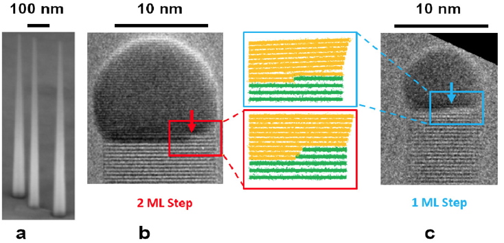 Figure: (a) ZnTe nanowires grown in our MBE cluster; (b) Nanomax image showing the gold seed at the top of the ZnTe nanowire, with a two-monolayer step at the interface; the step (indicated by the arrow) propagates from right to left; (c) idem, with a one-monolayer step. The schemes in-between display the Au atomic planes (in yellow) and the ZnTe planes (in green) for the two configurations.