Graphene is not an intrinsic superconductor but can become superconducting by proximity effect when it is intimately connected with a superconductor. In such a situation, new behaviors are expected in this two-dimensional ballistic system where electrons are described by a relativistic equation. However, the good quality of the interface between graphene and a superconductor together with the cleanliness of graphene on a large scale, remain very challenging and yet a key factor to study the ballistic superconducting proximity effect. To overcome this issue, we developed a very efficient way to strongly couple graphene to a superconductor, by growing it directly on top of rhenium, which shows superconductivity below 2K.
The graphene monolayer has been grown by a chemical vapor deposition process in a UHV chamber on epitaxial rhenium thin films of 30 nm thickness. The lattice parameters mismatch between graphene and Rhenium gives rise to a so-called moiré pattern that we characterized by scanning tunneling microscopy (STM, see figure below) and simulated with
ab initio calculations. Spectroscopic measurements performed at 50mK revealed that the density of states around the Fermi energy is position dependent on the moiré and highlighted a homogeneous superconducting state of the graphene layer, well fitted by the standard Bardeen-Cooper-Schrieffer (see figure below). All our results demonstrate a very good interface between graphene and the superconducting rhenium substrate, turning our system into a building block to design hybrid superconducting nanostructures, where the good transparency of the superconductor-normal metal interface is of primary importance.
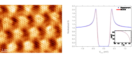
Left: STM image with atomic resolution showing the moiré superstructure due to the mismatch of the lattice parameter of graphene and Rhenium.
Right: Normalized differential tunneling conductance measured at 50 mK (blue dots). The local density of states displays a superconducting gap. The red curve is a BCS fit.
Collaborations:
Johann Coraux and Laurence Magaud, Néel Institute, CNRS Grenoble
Bruno Gilles, SIMAP, INP Grenoble
Project: ANR-BLANC SIMI10-LS-100617-12-01, SUPERGRAPH
Nanosciences Fondation grant SuperNanoCharac, DISPOGRAPH
European Project FP7-NMP-2009-SMALL-3 GRENADA