At low temperature, semiconductor quantum dots (QDs) are very efficient single-photon emitters. More particularly, the fundamental optical transition of a single InAs QD emits single photons at a wavelength around 950nm. However, the large refractive index (around 3.5) of the semiconductor matrix surrounding the QD strongly limits the amount of light that escapes from the device. Using a lens, one typically collects only 1% of the photons emitted by the QD.
Until now, the best solution to collect more photons was to insert the QD in a resonant optical microcavity. Due to several limits of this approach (see inset), we have chosen to locate the QD in a new, non-resonant, electromagnetic environment: namely, a GaAs photonic wire (Figure 1). This structure is a semiconductor waveguide of circular section that guides only a single optical mode. Thanks to the large refractive index of GaAs, this mode can be confined very tightly to a wire having a 200nm diameter. In addition, the non-guided modes are very efficiently screened by the structure. As a consequence, the emission of a QD located close to the wire axis is almost completely funneled into the guided mode.
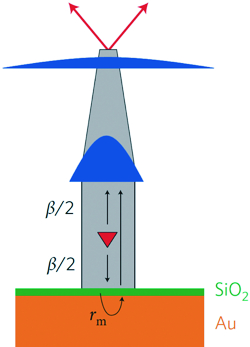
Figure 2: Sketch of the operation principle of the photonic nanowire. Half of the QD emission is directed towards the bottom where it is integrally reflected by the Au/SiO2 mirror. The cone at the top of the nanowire progressively releases the optical guided mode, sketched as blue surfaces.
The next challenge, solved with theoreticians at the Institut d’Optique (France) and DTU Fotonik (Denmark), is to efficiently collect the guided photons with a lens positioned above the wire. First, one has to avoid the loss of the photons emitted toward the bottom of the wire. To reflect them, we have inserted below the wire a mirror which consists of a gold layer topped by a thin (11nm) silica layer. The second issue concerns the wire top facet: as it is quite small (200nm diameter), the light coming out of this facet is strongly diffracted beyond the collection cone of the lens. Our solution is to sharpen the tip of the wire so as to progressively release the mode in the air as it travels toward the wire top. Being more extended when it leaves the wire, the mode radiates with more direction and can be collected efficiently.
We have fabricated such a source in the PTA and Leti/DOPT clean rooms. Under pulsed optical pumping, it features a very clean, single photon emission: less than 1% of the emission consists of multiple photons. Moreover, the overall efficiency reaches a record value of 72%. Beyond any significant progress, as compared to the state of the art, this non-resonant approach can be applied to spectrally broad single-photon emitters. Thus, it could be implemented to improve the efficiency of room-temperature single-photon sources, for instance by inserting a single colored center inside a diamond photonic wire.
Limits of microcavities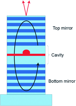
Up until now, the insertion of a single QD in a resonant optical microcavity was the most efficient way to increase the collection of the light emitted by the QD. A typical optical cavity consists of two mirrors facing each other; it is said to be resonant with the QD if the distance between the mirrors is an integer multiple of the QD emission wavelength. In these conditions, the QD spontaneous emission rate into the cavity mode is enhanced (Purcell effect), and the light emission is redirected perpendicularly to the mirror.
What are the limits of this approach? As the photons spend some time in the cavity bouncing back and force between the mirrors, they “feel” all fabrication defects (for instance a corrugation of the surfaces in a micropillar cavity) and can thus be scattered in arbitrary directions. These scattered photons are lost, and the efficiency of sources based on this principle presently attain a maximum of 40%. Besides, this approach also requires a resonance condition between the QD and the optical mode, which complicates fabrication. Finally, the emitter should be spectrally narrow when compared to the cavity resonance linewidth, thus limiting this approach to low temperatures for solid-state emitters.