The most recent microprocessors are made of almost a billion transistors. The control of the characteristics (values of the voltages which switch the transistors between the « on » and « off » states) of each transistor is essential. The number of dopant atoms inside the channel of these transistors has reached such a small value that each of them influences the transistor’s behaviour. In order to study their influence, in collaboration with LETI/D2NT, we have made transistors with an extremely small volume channel, which only contains 5 dopant atoms (in this case, arsenic) on average (Figure 1).
Uncovered at low temperature The consequence of the presence of a single dopant in the channel is revealed by measuring the conductance between the drain and the source, as a function of the gate voltage Vg (Figure 2) at very low temperature. When the transistor is cooled down below 4K, we observe very narrow conductance peaks. These peaks broaden as the temperature increases, until fully overlapping at room temperature. They are due to resonant quantum tunnelling, which involve an arsenic donor in the channel. By having measured several tens of nominally identical devices, we have shown that the spread of several orders of current magnitude for voltage values lower than the nominal threshold value (-0.5 volt), is due to the presence or absence of dopants in the channel. Hence, a single arsenic dopant dramatically modifies the threshold voltage and the current, in the off state, even at room temperature.
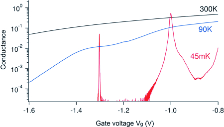
Figure 2: Drain-source conductance as a function of the gate voltage for different temperatures. At low temperature, the first two peaks associated with two arsenic dopants are clearly observed. They broaden at high temperature and are responsible for the anomalously high current level, which is observed at such a small gate voltage. In the absence of dopant in the channel, the conductance would vanish for these voltage values.
Influence of the dopant location The value Vg at which a peak is observed is associated with the ionisation energy of the corresponding dopant,
i.e., the energy dispensed for the release of the electron. One notices that it is much larger for a dopant located near the oxide layer than when it is close to the gate. This is an electrostatic effect related to the image charge generated in the oxide, an effect which is theoretically documented. Our work shows the importance of improving the doping techniques. It also suggests that the single dopant, a quantum object by essence, can be individually addressed and with a minimum consumption of energy.
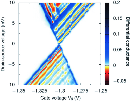
Figure 3: Signature of a dopant observed in the channel of a nanoscale transistor at 100 mK. The gate voltage Vg ≈ -1.3V corresponds to an ionization energy of 110 meV, which is as high as twice the value in silicon (54 meV). The lines seen in this conductance map come from the atomic roughness at the source-channel and drain-channel interfaces.