A collaboration with Institut Néel (Grenoble)
In the development of graphene based electronic devices a lot of care is usually taken in order to preserve its outstanding
electronic properties. The quality of the graphene itself and the absence of defects or contamination are at the heart of most
of the researches. A lot of efforts are also focused on the choice of the substrate which is known to play an important role. However,
these devices require the presence of metallic electrodes to connect it to the outside world. Very little is known about the impact of
these metallic contacts on the properties of graphene. In particular, the mechanical stress that is induced in graphene during the
metal thin film deposition can greatly influence the graphene properties near the contact and further limit the electronic mobility
of the global device.
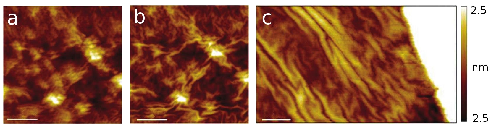 Ripples observed at different bias bias voltages Vb, 0.1 V and 0.5 V respectively, 250 nm away from the graphene-metal interface (a and b).
Closer to the metal layer (c), a strong buckling of graphene can also be observed which leads to wrinkles parallel to the graphene-metal interface.
This strained graphene display a gap of a few hundred of millivolts in the local electronic density of states
Ripples observed at different bias bias voltages Vb, 0.1 V and 0.5 V respectively, 250 nm away from the graphene-metal interface (a and b).
Closer to the metal layer (c), a strong buckling of graphene can also be observed which leads to wrinkles parallel to the graphene-metal interface.
This strained graphene display a gap of a few hundred of millivolts in the local electronic density of states
STM imaging and tunneling spectroscopy of graphene performed in the vicinity of a metallic film deposited on top of it, reveal intense
shear stress. They lead to a series of mechanical instabilities which take different morphologies as one comes closer to the metal
contact edges. In particular, for positions less than a micron away from the contact, we show a bias dependent rippling of graphene which
is enhanced by increasing the transverse electric field induced under the tip of the STM. (Fig. 1A & 1B) These ripples are suspended areas of
graphene which can be easily pulled by the STM electric field and therefore manipulated at will. In extreme situations, we observed a strong
buckling of graphene nearby the metallic electrode. (Fig. 1C)
In this case tunneling spectroscopy reveals a gap of a few hundred millivolts in the local electronic density of states in
graphene. This gap can be explained by the interplay of quantum confinement and Coulomb blockade.
More info in
Nanoscale DOI: 10.1039/C3NR02934D (2013).