 Context
The capability to integrate active and passive optoelectronic devices on a Si wafer is an essential paradigm in the quest for the development of low-cost and energy-efficient data communication, imaging, and quantum sensing technologies. To this end, a monolithic all-group IV semiconductor platform is at reach using direct band gap GeSn semiconductors.1 Over the last decade, tremendous progress was made in the epitaxial growth of GeSn, where a direct band gap material (i.e. high efficiency for the optical emission) is obtained at Sn contents of >9 at.%. Prototypes of GeSn photodetectors, lasers, and LEDs have been fabricated from the short-wave infrared (SWIR: 1.5-3 μm) to mid-wave infrared (MWIR: 3-8 μm) wavelengths.2,3 The main bottleneck with the GeSn technology is, however, the large number of structural defects that severely reduces the efficiency of the photonic devices made using GeSn. This prevents a wide scale adoption of GeSn photonics in favor of conventional, yet expensive III-V and II-VI semiconductor technologies.
Project
The growth of GeSn is commonly performed on Si using Ge as an interlayer in a chemical vapor deposition (CVD) reactor, hence with an industrial- compatible fabrication process. However, the lattice-mismatch between GeSn and the Ge/Si substrate leads to compressive strain in GeSn and plastic strain relaxation results in structural defects. Defects are a source of nonradiative recombination and largely contribute to the dark current of GeSn photonic devices, in turn strongly reducing efficiency.
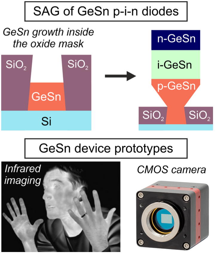
This thesis will overcome these challenges and develop the selective area growth (SAG) of defect-free GeSn p-i-n diodes from nanometer-size openings that are patterned into an oxide mask layer on Si. The SAG has proven to be a highly valuable approach for the integration of defect-free III-V semiconductors on Si,
4 with similar results that are now being explored in Ge.
5 The GeSn growth will be selectively confined in very small regions of the patterned oxide/Si wafer. In SAG reducing the lateral dimensions of the patterned oxide windows will strongly decrease the defect density in the epitaxially-grown GeSn layer through dislocation filtering. The unmatched crystalline quality of SAG GeSn will boost the efficiency of infrared optoelectronic devices and thus establish a robust, scalable monolithic infrared photonics platform using group IV semiconductor materials. Photodetector devices made of SAG GeSn p-i-n diodes will be fabricated as a template system to demonstrate the effectiveness of SAG compared to the existing GeSn technology based on unpatterned GeSn samples.
2
Competences to be acquired
(i) Epitaxial growth of Sn-based group IV semiconductors using CVD and molecular beam epitaxy (MBE) tools.
(ii) Structural characterization of the SAG materials down to the atomic-level.
(iii) Fabrication of infrared photonic devices in a cleanroom facility.
(iv) Optoelectronic characterization of materials and devices.
Required skills
Background in solid-state physics and materials science, interest in performing experiments in the lab, working in a collaborative team, and contributing to international collaborations.
Starting date
By the 1st October 2024.
PhD fundingThesis funded by Initiatives de Recherche à Grenoble Alpes (IRGA).
SupervisorDr. Simone Assali (CEA-IRIG/PHELIQS, Grenoble).
Further reading 1. Monolithic infrared silicon photonics: The rise of (Si)GeSn semiconductors.
2. High-Bandwidth Extended-SWIR GeSn Photodetectors on Silicon.
3. Electrically injected GeSn lasers with peak wavelength up to 2.7 μm.
4. GaAs nano-ridge laser diodes fully fabricated in a 300 mm CMOS pilot line.
5. Coherent Hole Transport in Selective Area Grown Ge Nanowire Networks.