Photonics on silicon is considered as a major tool for optical data communication, signal processing and detection applications. The fabrication of photonic circuits is based on processes and protocols similar to CMOS (complementary metal-oxide-semiconductor) technology and is therefore limited to a well-defined set of materials, preferably from the Group IV atomic column, such as silicon. However, the key element, a laser source with fully integrated electrical control on Si, is still missing and is considered as a challenging milestone in the field of Si-photonics. Germanium, thanks in part to its CMOS compatibility, is an excellent candidate.
Fully integrated light sources in microelectronics are the missing building blocks of photonics on silicon. Silicon, like germanium, is not well adapted to the emission of light in its natural form, due to the indirect nature of its
gap. However, germanium has long been considered as a promising laser material for silicon-based
optoelectronics due to its compatibility with CMOS-type industrial processes. Its
band structure can be tailored to trigger direct transitions, (essential property for interband semiconductor lasers) either by deforming the Si mesh or by alloying it with another group IV element, namely Sn.
A team of researchers from IRIG, in collaboration with the Optics and Photonics Department and the Technology Platform Department of CEA-Leti, obtained a mid infrared laser emiting in the 2.7 to 3.2 µm range and up to 230 K, in a nanostructure made of a Germanium-Tin alloy
[1]. This first result therefore paved the way for photonic sources that could be integrated on a silicon chip. In a new study conducted in collaboration with the Paul Scherrer Institute (PSI) in Switzerland
[2], they were able to obtain a laser emission using the second approach from pure but very strongly deformed germanium. Finally, by combining these two approaches, i.e. by deforming the active zone of the microlasers in GeSn, the Grenoble researchers succeeded in obtaining a laser emission over a very wide frequency range and at an operating temperature reaching 273 K, very close to the symbolic hurdle of room temperature
[3]. The major difficulty of this approach lies in the ability of producing a tin-rich alloy while preserving its high crystalline quality (no crystalline defects that would annihilate the laser effect), as well as being able to apply a high stress on the area to obtain a tunable laser emission. Using a nanofabrication process developed over several years, researchers have succeeded in obtaining an alloy containing up to 16 % tin and showing a strong direct gap character.
With this first result at 273 K, the team is already well beyond the 90 K obtained in 2015 by the pioneering team of the GeSn laser. The objective now is to optimize the system to move towards room temperature operation to make it usable for photonic applications.
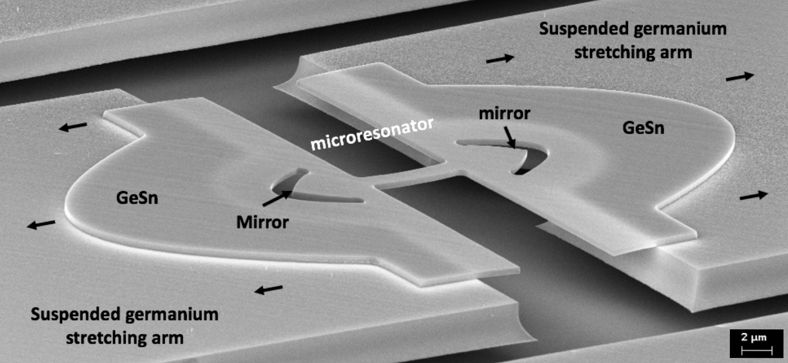
SEM image of a GeSn microlaser with control of uniaxial deformation in the active zone. The device, fully suspended, includes two germanium tension arms pulling on a central GeSn area. In this area, we can distinguish the areas of anchorage to the arms located on either side of the GeSn plot, while the area of the GeSn entirely in the air, and where the resonator is located, consists of a waveguide (bridge) and two mirrors ensuring the reflection of light.
© CEA-IRIG