New ultraviolet (UV) light-emitting diodes (LEDs) have been commercially available for only a few years and are actually used for various applications such as fluorescence, polymerization, catalysis, skin disease treatment and UV disinfection. Researchers at PHELIQS have recently succeeded in miniaturizing this type of LED at micrometer scale to fabricate UV microLEDs, based on nanowire with a diameter 100 times smaller than a hair. This new device paves the way for new applications, such as UV pixel displays for biological detection and on-demand photolithography, or the fabrication of flexible UV-LEDs.
The researchers, in collaboration with the Neel Institute, have developed an alternative approach using nanowires to fabricate UV microLEDs. This “nanowire” approach dramatically reduces the effect of dislocations within the material, increases the UV emissive surface area and improves UV light extraction. Based on GaN nanowires, the UV-LED structure is epitaxially grown in a core/shell geometry, integrating a UV source inserted into an AlGaN diode (p-n junction). Two types of active structures capable of emitting in the UV-B range have been successfully developed: 1) GaN quantum wells with a thickness of only 0.7 nm, corresponding to 3-4 atomic planes (monolayers) of GaN, or (2) a GaN/AlGaN superlattice to modulate the crystal composition at the scale of only 2 monolayers (referred to as a digital alloy). For both active structures, electrical contact was made on the single nanowire to accomplish UV microLEDs. By applying an electrical voltage, intense UV-B emission at 310 nm is achieved!
In the semiconductor field, these pioneering works on the development of miniaturized UV-LEDs with core-shell nanowire represent a significant advancement in the field of UV light sources and nanophotonics. Today, researchers of IRIG target to design UV-C LED based on nanowires and hope to make flexible UV LEDs on large surface from an assembly of these nanowires. The very first results on flexible UV-LED look particularly promising and will soon be presented at the 14th ICNS conference.
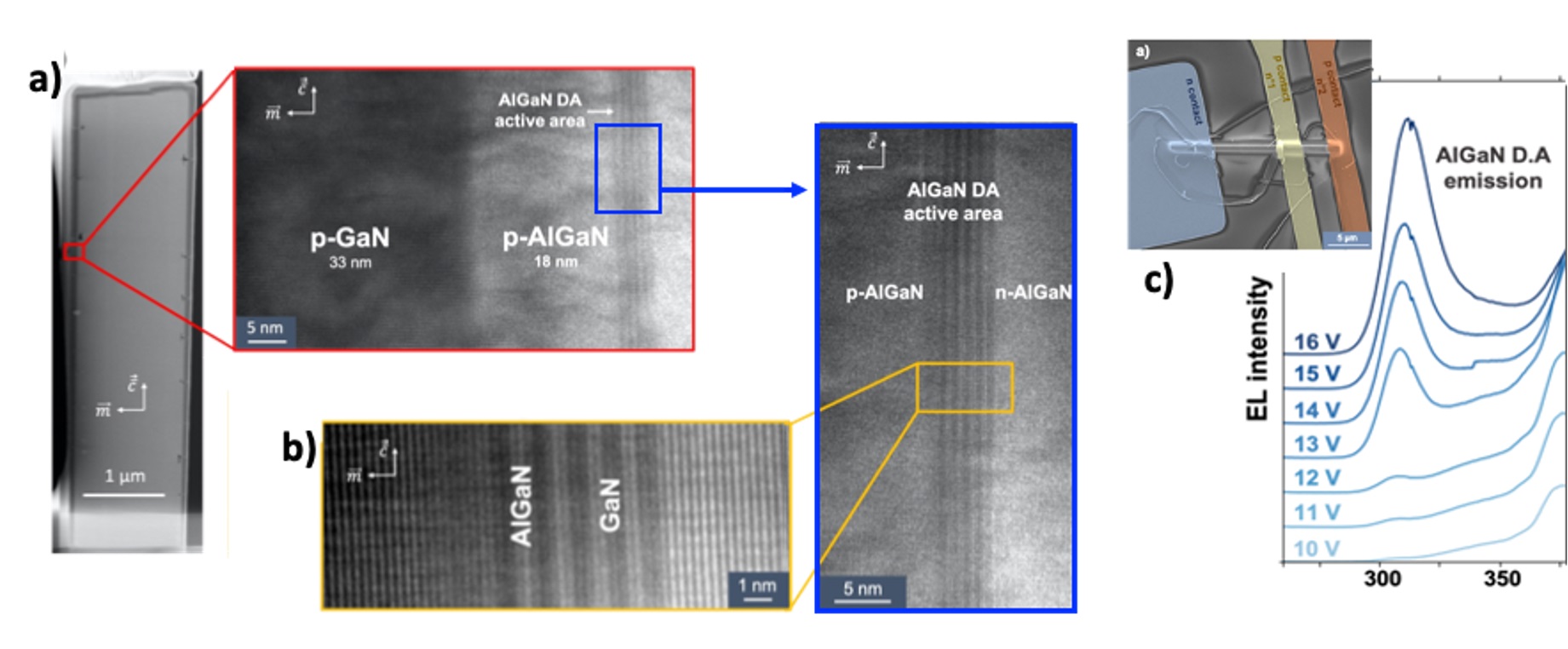
Figure: (a) TEM Image of a nanowire with a core-shell UV LED structure. (b) TEM Image of the UV active zone consisting on a GaN/AlGaN superlattice (called DA for digital alloy), where each layer is 2 atomic monolayers thick. (c) Emission at 310 nm from the polarized nanowire UV-LED between 10 and 16 V.
Fundings: Program Initiatives de Recherche Stratégiques (IRS) of IDEX Université Grenoble Alpes (ANR-15-IDEX-0002) and the ANR project called HARALN (ANR-22-CE51-0032-01).